
Review Article | DOI: https://doi.org/10.58489/2836-5127/011
*Corresponding Author: Alla Srivani
Citation: Alla Srivani, Gurram Vasanth, GVS Subbaroy Sharma, Srinivasa Rao, P Ramesh, A Raghavendra, G Krishna Kumari, (2023). SEM Imaging for Advanced Bio Materials. Journal of Radiology Research and Diagnostic Imaging. 2(2). DOI:10.58489/2836-5127/011
Copyright: © 2023, Alla Srivani, this is an open access article distributed under the Creative Commons Attribution License, which permits unrestricted use, distribution, and reproduction in any medium, provided the original work is properly cited.
Received: 30 January 2023 | Accepted: 06 February 2023 | Published: 10 February 2023
Keywords: sem, bio imaging, bio materials
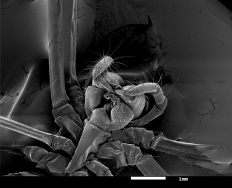
Scanning electron microscopy (SEM) is one of the popular methods for imaging the microstructure and morphology of materials. In an SEM, a low-energy electron beam hits the material and scans the surface of the sample. As the beam reaches and enters the material, various interactionsoccur that result in the emission of photons and electrons from or near the sample surface. To produce an image, the received signal produced by the electron-sample interaction is detected with different types of detectors, depending on the her SEM mode used. There are various his SEM modes for characterization of materials including biomaterials. B. X-ray imaging, secondary electron imaging, backscattered electron imaging, electron channeling, Auger electron microscopy.
Human eye can distinguish between two points in space that are 0.2 mm apart without an additional lens. This distance is called the resolving power or resolution of the eye. A lens or array of lenses (microscope) can be used to extend this distance so that the eye can see points much closer than 0.2 mm. Modern light microscopes have a maximum magnification of about 1000x.
The resolution of a microscope is limited not only by the number and quality of lenses, but also by the wavelength of light used for illumination. Specifically, white light is in the wavelength range of 400 to 700 nano meters (nm),with an average wavelength of 550 nm in this range. This gives a theoretical resolution limit (not visibility) for optical microscopy in white light of about 200–250 nm. The spotsin are still distinguishable. The image on the right shows that the two points are so close together that the central points overlap.
Scanning electron microscopy (SEM) is one of the most widely used instrumentation methods for studying and analyzing imaging micro- and nanoparticle characterization of solid objects. One of the reasons SEM is preferred for particle size analysis is its resolution of 10 nm, or 100 Å. Advanced versions of these instruments can achieve resolutions of around 2.5 nm (25 Å) (Goldstein, 2012). The instrument can also be used in conjunction with other related energydispersive X-ray microanalytical techniques (EDX, EDS, EDAX) to determine the composition or orientation of individual crystals or features.
A tungsten incandescent lamp or a field emission gun is generally used as an electron source. Field emission guns require ultra-high vacuum conditions (10-10 to 10-11 Torr) to keep the tip free of impurities and oxides (Pathak and Thassu, 2016). The electron beam is accelerated by a high voltage system "20 kV", and after passing through an aperture and an electromagnetic lens it is focused. The beam scans the sample surface using scanning coils. After SEM-type generation, an image is generated from the signal from the area of beam-sample interaction. Backscattered electrons and secondary electrons emitted by the sample above the vacuum level are collected by anappropriately positioned detector (Hafner, 2007). Focusing an area at higher magnification levels (>100kX) enhances surface topography analysis of samples with the highest spatial resolution.
SEM is a versatile instrument that can visualize and analyze almost any material. This makes it the perfect “workhorse” for forensic labs. The applications of SEM-EDS are myriad. SEM has typically been applied in conjunction with EDS in forensic research and cases involving paint, GSR, glass, metal, bone, minerals, soil, building materials, dental restorations, pollen, tape, cuts, explosives, etc. rice field.
SEM-EDS is very useful for forensic investigations with its ability to visualize surfaces, position the beam for analysis, and generate elemental and chemical information about heterogeneous constituents of the sample.
Some examples show multiple uses for this device. In an attempt to identify bullet wipers from wounds, pork ribs with intact musculature were shot with .45 caliber ammunition from a range of 1 to 6 feet. Unexpectedly, the shot was fired from a distance of 6 feet, and after processing the tissue and bone for viewing in his conventional SEM.
ACCELERATION VOLT AGE (KV) | SPOT SIZE (nm) | Z height distance (mm) |
5 10 15 | 5 10 15 | 8 10 20 |
The GSR was found deep within the wound tract within the bone. This finding means that the method may allow analysts to distinguish gun trauma from other confusing types of trauma.
The ability to visually locate and essentially identify individual her GSR particles, which are only a few micrometers in size, is otherwise impossible. In another example of wound assessment, SEM was used to visualize tool his marks on bone and compare them.
Bone and associated tissues are excellent media for recording and documenting tool marks such as those made by knives, allowing conventional comparison of tool marks.
We can also determine the direction of the cut and whether it was cut with fresh or dry bone. This is an important distinction in forensic examination.A scanning electron microscope (SEM, Tescan VEGA II SBH) was used to observe the morphology of the titanate nanowires.
In this study, an X-ray diffractometer (XRD, Rigaku MiniFlex II) was used to analyze the crystal structure of titanate nanowires. For elemental composition analysis, thetechnique of energy dispersive X-ray diffraction (EDX) (Bruker AXS Microanalysis GmbH Berlin, Germany, EDX system) was used. All results for the above characterization parameters (SEM, XRD, and EDX) have been previouslydescribed in detail.
Biomaterial approaches to restoring tissues and organs by exploitation different bio fabrication methods andmaterials, specializing in recent advances within the field of tissue engineering and regenerative medicine. Papers cowl the planning of biomaterials and devices to be applied in vivo and in vitro, and a spread of topics regarding somatic cell biology, biomaterials and technological approaches. Specific topics embrace the generation of recent useful internalorgan substitutes, enhancements in the bone repair
process, neural tissue formation, a pioneering model of viscus fibrosis, and therefore the creation of a completely unique vein valve prosthesis. This multi-disciplinary approach highlights however the various characteristics of biomaterials and devices are to blame for the promotion of cell integration, and ultimately new tissue formation. This issue may be a must-read for biomaterial scientists, tissue engineers, clinicians, in addition as somatic cell biologists concerned in basic analysis and its applications.
Lithium-ion batteries (LIBs) are important energy-storage devices in fashionable society. However, the performance and value are still not satisfactory in terms of energy density, power density, cycle life, safety, etcetera to more improve the performance of batteries, ancient “trial-and-error” processes need a massive variety of tedious experiments.
procedure chemistryand computing (AI) will considerably accelerate the analysis and development of novel battery systems. Herein, a heterogeneous class of AI technology for predicting and discovering battery materials and estimating the state of the battery system is reviewed. sure-fire examples, the challenges of deploying AI in real-world scenarios, and an integrated framework are analyzed and outlined.
The progressive analysis concerning the applications of millilitre within the property prediction and battery discovery, as well as solution and conductor materials, are more summarized. Meanwhile, the prediction of battery states is additionally provided.
Finally, varied existing challenges and also the framework to tackle the challenges on the further development of machine learning for reversible LIBs are proposed.